Atomic layer deposition is a methodology for extending thin films for a broad gamut of applications. It is a singular alternative of the chemical vapor deposition methodology, where gaseous reactants are inaugurated into the reaction chamber for establishing the wanted material through chemical surface reactions. The atomic layer deposition market size is expanding as the forerunners are palpitated alternatively, one at a time, and segregated by inert gas removal so that gas phase reactions can be avoided.
The global atomic layer deposition market was valued at USD 1.90 billion in 2022 and is expected to grow at USD 6.01 billion with a CAGR of 12.2% during the forecast period.
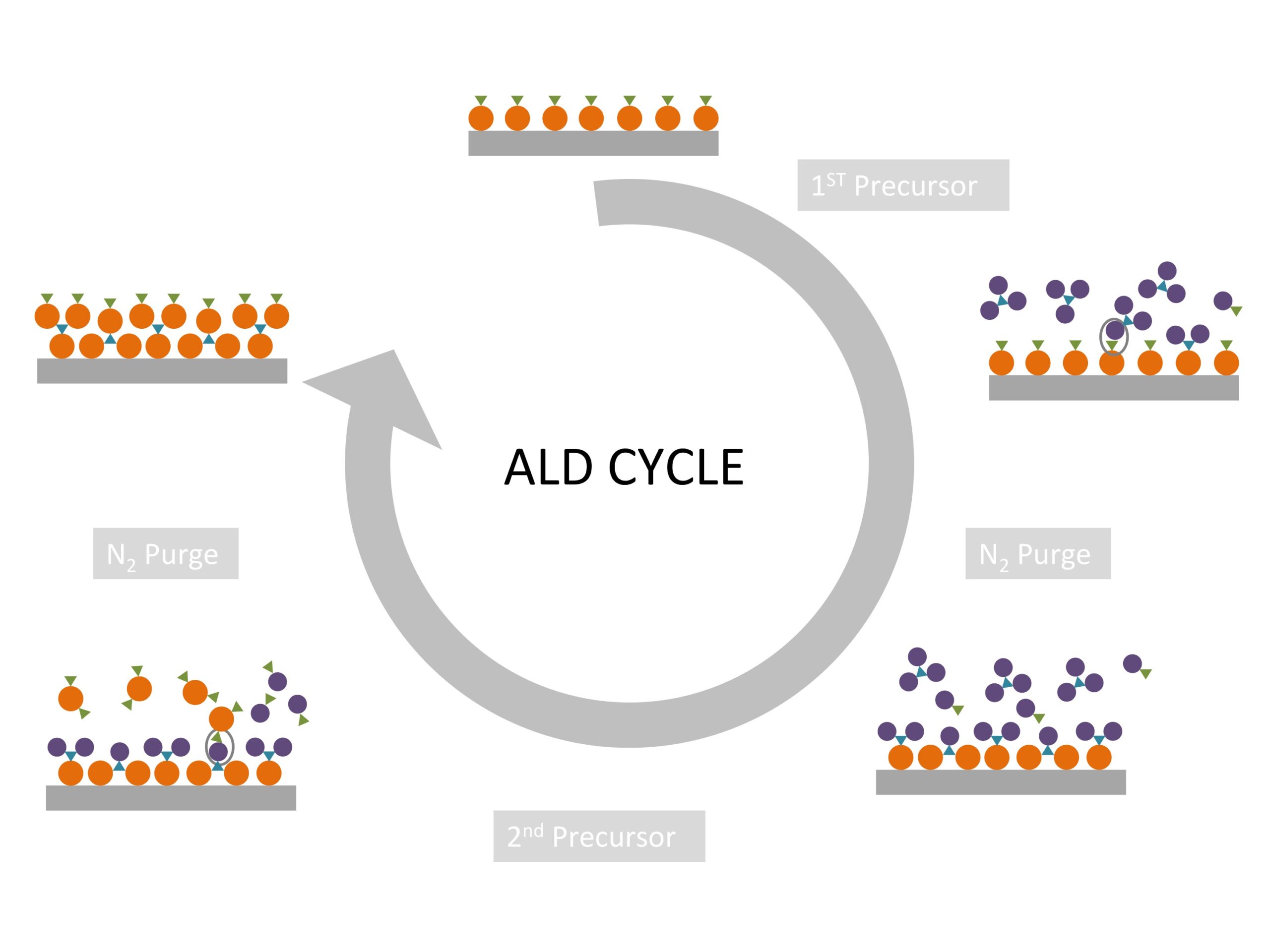
What Are the Types of Atomic Layer Depositions?
- Thermal ALD: This includes a binary procedure with two reactants, A and B. The first reactant, A, is injected into the ALD chamber. The wafer is treated, and then chemistries are removed. Then the second reactant, B, experiences the same step.
- Plasma ALD: In this kind of ALD, the responses are plasma-based, a technique used in low-temperature applications.
Configurations for Atomic Layer Depositions Tools
- Furnace or batch systems: These systems manage a host of wafers and authorize thicker films. Utilized by DRAM makers, batch systems are proportionately speedier, but there is an exchange concerning constancies.
- Single wafer ALD tools: These are used in applications where uniformity specs are attenuated and compact. Single wafer, which is utilized to sublimate elevated K dielectrics in logic, are also time-dependent systems. In time-based instruments, the reaction occurs in a chamber for a set or provided time.
- Spatial ALD tools: These are mini batch systems. An aggregate of wafers is positioned in the system. The wafers convey to several territories. At each territory, a reactant is pushed into the chamber. The wafer is then prepared and then is located to subsequent territory.
Growth Propellers
The growing demand for microelectronics and consumer electronics because of initiation to several reasonable and lightweight instruments involving capacitors, transistors, diodes, inductors, resistors, and several others that are being notably utilized in the making of tablets, mobile phones, electronic toys, and laptops among others are the prominent factors that are anticipated to push the growth of the global market.
Thermal ALD is the Governing Factor
The extensive usage of this kind of ALD methodology for settling aluminum accommodating molecules and escalated pervasiveness of the aluminum oxide film utilizing this methodology are amidst the prominent factors propelling the demand and growth of this segment. The atomic layer deposition market sales are soaring due to the growing consciousness in relation to several outstanding properties involving elevated steadiness of several substrates and simplicity of approach to the former materials are several other features chipping in the segment growth.
Topographical Reach
Asia Pacific: The market in this region was proliferating mainly due to the strong existence of prominent electronic makers in India, China, South Korea, and Taiwan and escalated government disbursement on advancing infrastructure to obtain scrutiny of spearheading market players to initiate their production potential in the region is the critical factors pushing the augmentation and the growth of the market.
North America: This region is likely to develop at a sizeable growth rate due to an uninterrupted rise in the demand for electric vehicles amidst people and escalating figures of solar energy projects and data centers structured across the US.
Recent Developments
In October 2022, Samco introduced Plasma Enhanced Atomic Layer Deposition system named “AD-800LP”. The new system R&D system is equipped with the ICP plasma, which enables stable discharge even in the high-pressure range.
Future Perception
The future possibilities for ALD are extremely encouraging. Several substances can be deposited utilizing ALD methodologies. The obtainability of several commercial ALD reactors persists to render ALD approachable for many workers exterior to the thin film growth section. In the atomic layer deposition market, the future should witness ALD to persists expand into contemporary fields and detect additional entreaties that benefit from its exact thickness regulation and conformity.